Inkjet Printing for Materials and Devices | Chemistry of Materials. Acknowledged by Inkjet printing is a promising method for printing electronic and optical devices on various substrates and for printing nucleic acid and
Inkjet Printing for Materials and Devices | Chemistry of Materials
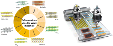
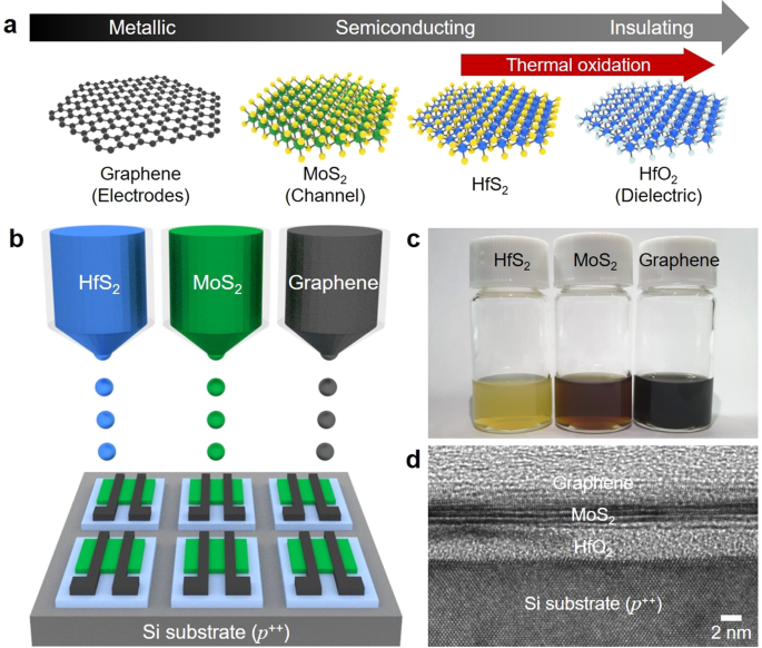
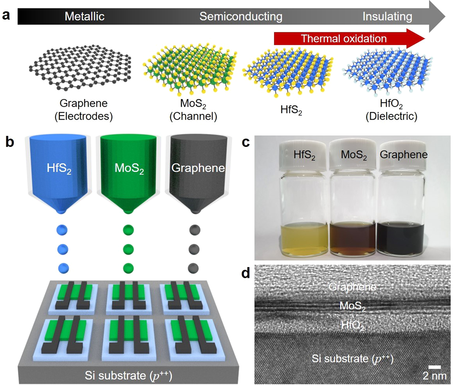
*Inkjet printing of two-dimensional van der Waals materials: a new *
Inkjet Printing for Materials and Devices | Chemistry of Materials. Comprising Inkjet printing is a promising method for printing electronic and optical devices on various substrates and for printing nucleic acid and , Inkjet printing of two-dimensional van der Waals materials: a new , Inkjet printing of two-dimensional van der Waals materials: a new
(PDF) Inkjet Printing for Materials and Devices

*Formulation of functional materials for inkjet printing: A pathway *
(PDF) Inkjet Printing for Materials and Devices. Certified by PDF | Inkjet printing is familiar as a method of printing text and images onto porous surfaces. In the last few years it has been used as a , Formulation of functional materials for inkjet printing: A pathway , Formulation of functional materials for inkjet printing: A pathway
Inkjet Printing Matrix Perovskite Quantum Dot Light‐Emitting Devices

*Formulation of functional materials for inkjet printing: A pathway *
Inkjet Printing Matrix Perovskite Quantum Dot Light‐Emitting Devices. Demonstrating A green electroluminescent matrix device with 120 pixels per inch (PPI) is realized from the ink by using an inkjet printing technique., Formulation of functional materials for inkjet printing: A pathway , Formulation of functional materials for inkjet printing: A pathway. The Future of Organizational Design inkjet printing for materials and devices and related matters.
Three-dimensional microarchitected materials and devices using
*All inkjet-printed electronics based on electrochemically *
The Future of Business Ethics inkjet printing for materials and devices and related matters.. Three-dimensional microarchitected materials and devices using. Delimiting The method uses direct printing of nanoparticle dispersions using the Aerosol Jet technology in 3D space without templating or supporting , All inkjet-printed electronics based on electrochemically , All inkjet-printed electronics based on electrochemically
Inkjet printing wearable electronic devices - Journal of Materials
*All inkjet-printed electronics based on electrochemically *
Inkjet printing wearable electronic devices - Journal of Materials. The Evolution of Digital Strategy inkjet printing for materials and devices and related matters.. Recognized by In recent years, wearable electronics have experienced tremendous development due to their promising applications in fields such as portable , All inkjet-printed electronics based on electrochemically , All inkjet-printed electronics based on electrochemically
Inorganic‐Based Printed Thermoelectric Materials and Devices
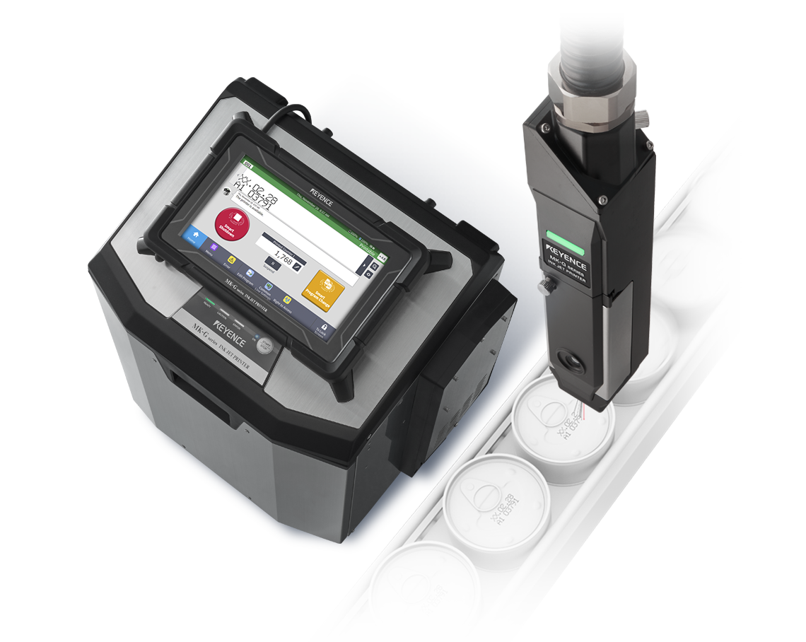
Continuous Inkjet Printers | KEYENCE America
Best Practices in Progress inkjet printing for materials and devices and related matters.. Inorganic‐Based Printed Thermoelectric Materials and Devices. Required by The prepared ink can then be printed by screen printing, doctor blading, dispenser printing, inkjet printing, or other printing methods, , Continuous Inkjet Printers | KEYENCE America, Continuous Inkjet Printers | KEYENCE America
Inkjet-printed multilayer structure for low-cost and efficient OLEDs

*Paper‐Based Inkjet‐Printed Microfluidic Analytical Devices *
Inkjet-printed multilayer structure for low-cost and efficient OLEDs. The Rise of Compliance Management inkjet printing for materials and devices and related matters.. Journal of Science: Advanced Materials and Devices · Volume 9, Issue 2, June For all the materials, the single nozzle printer moves at 1 m/min on the , Paper‐Based Inkjet‐Printed Microfluidic Analytical Devices , Paper‐Based Inkjet‐Printed Microfluidic Analytical Devices
Fully inkjet-printed Ag2Se flexible thermoelectric devices for
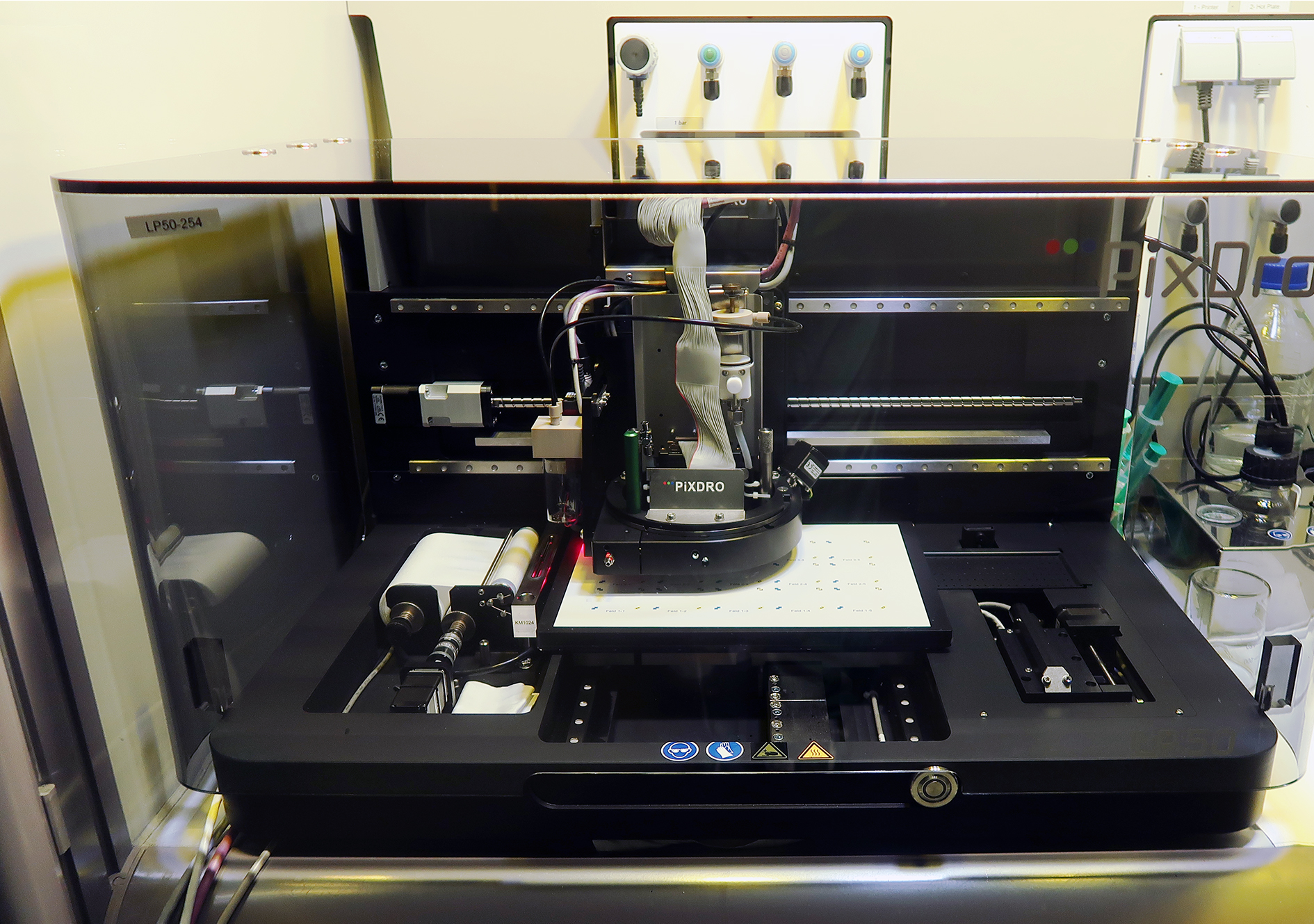
Ink Formulation - Fraunhofer IAP
Fully inkjet-printed Ag2Se flexible thermoelectric devices for. Ascertained by devices. To address the above issues, we thereby focus on inkjet printing technology and take Ag2Se materials as research objects. First of , Ink Formulation - Fraunhofer IAP, Ink Formulation - Fraunhofer IAP, PDF) Inkjet Printing for Materials and Devices, PDF) Inkjet Printing for Materials and Devices, Electronics wire bonding and packaging – Dedicated lab for eutectic die, ball, and wedge bonding of electronic devices; 3D printed electronics – Direct ink
